PCB Manufacturing Process: A Complete Guide from Raw Material to Finished Circuit Board
 Printed Circuit Boards (PCBs) are the foundation of modern electronic products, including power meters, consumer electronics, industrial controllers, automotive electronics, and communication equipment.
Understanding the PCB manufacturing process is essential for manufacturers planning to establish a new PCB factory or upgrade existing production capabilities.
In this article, we will walk through the complete PCB manufacturing process and introduce the key equipment used in each stage.
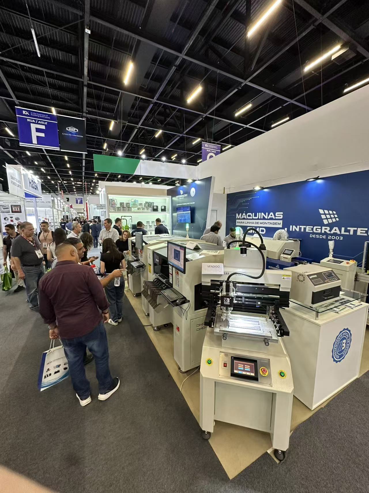
What is a PCB Manufacturing Line?
A PCB manufacturing line is a complete production system used to convert copper clad laminate (CCL) into finished printed circuit boards.
Typical PCB production includes:
-
Inner Layer Processing
-
Lamination
-
Drilling
-
Copper Plating
-
Pattern Transfer
-
Etching
-
Solder Mask
-
Surface Finishing
-
Electrical Testing
-
Final Inspection
The process starts with copper clad laminates.
Photoresist is applied to the copper surface and exposed using artwork or direct imaging equipment.
Purpose:
-
Create circuit patterns
-
Define electrical connections
Main Equipment:
-
Exposure Machine
-
Developing Line
-
Etching Line
[Insert Inner Layer Exposure Machine Image]
Step 2: Multilayer Lamination
For 4-layer, 6-layer and higher layer count PCBs, multiple core boards and prepregs are stacked together.
The lamination press applies heat and pressure to create a single multilayer board.
Main Equipment:
-
Lay-up System
-
Vacuum Lamination Press
[Insert Lamination Press Image]
Step 3: CNC Drilling
Holes are drilled according to PCB design data.
These holes later become electrical interconnections between layers.
Main Equipment:
-
CNC Drilling Machine
[Insert CNC Drilling Machine Image]
Step 4: Copper Plating
After drilling, conductive copper is deposited inside the hole walls.
This creates electrical continuity between layers.
Main Equipment:
-
PTH Line
-
Electroplating Line
[Insert Plating Line Image]
Step 5: Outer Layer Pattern Transfer
The outer layer circuit pattern is transferred onto the PCB.
Main Equipment:
-
Exposure System
-
Developing & Etching Line
[Insert Outer Layer Imaging Image]
Step 6: Solder Mask Application
Green solder mask is coated onto the board surface.
Functions:
-
Protect circuits
-
Prevent solder bridges
-
Improve reliability
Main Equipment:
-
Solder Mask Coating Machine
-
UV Exposure System
[Insert Solder Mask Process Image]
Step 7: Surface Finish
Different finishes can be applied:
-
HASL
-
Lead-Free HASL
-
ENIG
-
OSP
-
Immersion Tin
-
Immersion Silver
The choice depends on product requirements.
Step 8: Electrical Testing and Inspection
Every PCB must be tested before shipment.
Main Equipment:
-
Flying Probe Tester
-
AOI System
-
Electrical Tester
[Insert AOI Inspection Image]
PCB Manufacturing Line Solutions
Whether you are producing 2-layer, 4-layer, or 6-layer PCBs, selecting the right equipment configuration is critical for productivity and quality.
AscendSMT provides complete PCB manufacturing line solutions, including:
-
Wet Process Line
-
Lamination Equipment
-
Drilling Equipment
-
Surface Treatment Equipment
-
Inspection Systems
Contact us to discuss your production requirements and receive a customized PCB factory solution.